 Beginner Why long-term crypto holders borrow against assets instead of selling A strategic guide to liquidity management, capital preservation, and the real tradeoff between selling and borrowing crypto Open guide
 GMO to Release World’s First 7nm Bitcoin Mining Card

Photo by Alexandre Debiève on Unsplash
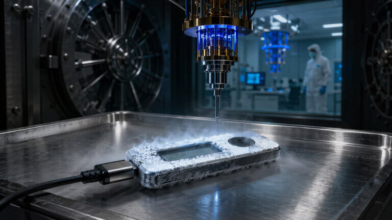
Japan’s GMO Internet Group officially announced the June 7th release of its new Bitcoin mining card— “GMO Miner B2”, marking a new era of powerful, energy-efficient processing units as the world's first 7nm consumer mining card.
This announcement highlights the ASIC arms race for producing more powerful and energy efficient mining rigs against companies like Samsung, Intel, and Globalfoundries.
The Next Milestone for Processor Architecture

The current, most popular Bitcoin mining card, the Antminer S9, utilizes Bitmain’s proprietary BM1387 16nm chip to provide 14 TH worth of hashing power.
Meanwhile, the 10nm DragonMint T1 features a Samsung made T1558 chip pushing 16TH with the addition of ASIC boost for greater power efficiency.
Though these chips provided Samsung with a significant revenue boost, they only show incremental performance gains over their last generation counterparts.
The upcoming 7nm chips are estimated to contain 20+ billion transistors and will offer up to a 40% performance gain, or over 65% power reduction compared to their 16nm rivals. The higher density of the chips will also allow for a 20% area size reduction, resulting in smaller, lighter and more powerful machines.
GMO appears to have surpassed competitors when it comes to 7nm dyes. Samsung expects to begin production in June while TSMC – already in production, is slated to be released later this quarter in AMD and Nvidia GPUs.
Intel Lags Behind Competition
During the JP Morgan Global Technology Media and Communications Conference this year, Intel announced the delay of their 10nm production until 2019 due to yield issues caused by their multi-patterning technique. This will undoubtedly affect the chip maker's 7nm development schedule unless an unforeseen breakthrough allows them to leapfrog the 10nm lithography.
Transitioning to 7nm introduced an entire suite of technical manufacturing issues that accompany the move from deep ultraviolet immersion lithography to extreme UV. The jump in dye size requires a jump in emitted laser wavelength, moving from 193 nm down to 13.5 nm.
Aside from increasing in power to produce these wavelengths, manufacturers also introduced pellicle and vacuum chambers to the new fabrication units to mitigate newly found issues.
GMO’s first generation of 7nm chips anticipates providing the company with a substantial advantage for the latest production of mining cards. As the architecture matures, many expect the new generation of silicon to provide consumers with increased performance.
GMO will host a customer information session in Shibuya, Tokyo, on June 6th and the new units are expected to be shipped at the end of October 2018.


